
| Broadband Monitoring Simulation tool of OptiLayer allows you to perform computational experiments simulating deposition processes in vacuum chambers equipped with broadband monitoring devices.
A six-step dialog is used to specify parameters of deposition process and monitoring device, to run computational experiments, and to analyze their results. OptiLayer simulator allows specifying major deposition parameters causing errors in the course of the deposition process:
|
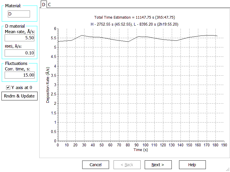 Fig. 1. OptiLayer visualizes computational manufacturing experiments. Fig. 1. OptiLayer visualizes computational manufacturing experiments. |
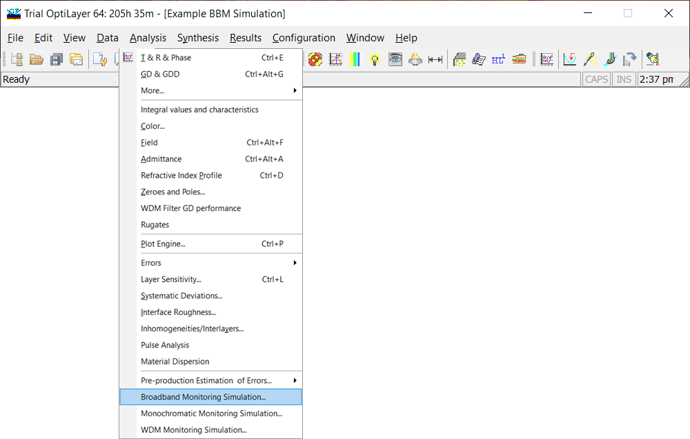
Fig. 2. BBM option. |
BBM simulator of OptiLayer is available through
Analysis –> Broadband Monitoring Simulation Due to high computational efficiency and multithreaded computations, OptiLayer allows you to perform hundreds of simulated deposition runs in a very short time. The BBM Simulator exploits the same control algorithm for determining termination times as DLL OptiReOpt. This algorithm is extremely efficient from a computational point of view and due to this fact works very fast. This allows us to use for computational experiments internal time scale in which time runs much faster than in reality. |
| In the six-step dialog you can specify simulation parameters.
At the first step of the dialog (Fig. 3, left panel) you should specify estimated mean values of deposition rates (Mean rate, A/s) and expected rms fluctuations of deposition rates (RMS, A/s) for all layer material that are used in the analyzed design. Typically dependencies of deposition rates on time are stationary random processes with correlation times of several seconds. The Fluctuations panel allows you to specify correlation times of deposition rates (Corr. time, s) and their rms (RMS, s). The Rndm & Update button enables previewing simulated dependencies of deposition rates on time. Rates corresponding to different materials can be selected with the help of tabs at the top of the window. Each time the Rndm & Update button is pressed a new set of simulated data is generated. At the second step (Fig. 3, right panel) it is possible to specify offsets of refractive indices of layer materials (both systematic and random ones) and the level of systematic inhomogeneity of design layers. Important: If it is necessary to consider complicated difference of refractive index from the theoretical one, it is possible to specify a different material from the Layer Material database for the same design abbreviation. In the middle part of the dialog, it is possible to exclude some design layers from the BBM procedure. In some cases it may be desirable to monitor specific layers by other means, for example, by time or with the help of quartz crystal monitoring. RMS Relative Thickness Error column allows you to specify the level of errors of these supplementary types of monitoring. Also it is possible to specify Mean shutter delay value and Shutter delay RMS, also affecting the quality of deposition process. |
|
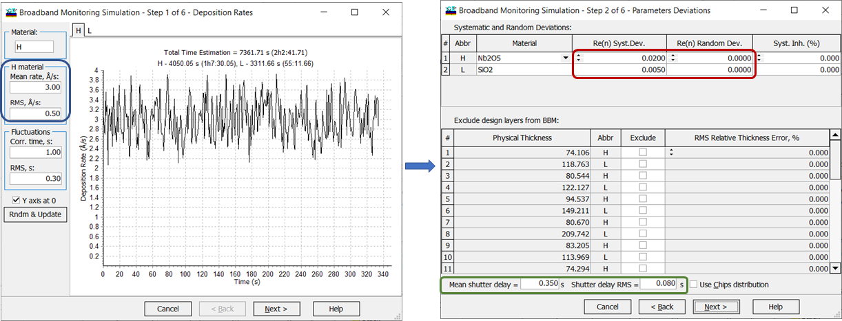
Fig. 3. Left panel: Step 1 of the BBM Simulator; Right panel: Step 2 of the BBM Simulator. Refractive index offsets are specified. |
|
|
At the third step of the dialog (Fig. 4, left panel), you should specify parameters of a simulated on-line monitoring device in accordance with those of a real monitoring device. The type of spectrophotometric measurements (reflectance or transmittance) is specified in the upper entry field. The next field is used to specify the Incident angle. Time interval between on-line data scans is specified in the Scan interval entry field. The Band panel is used to set lower and upper boundaries of the spectral region of on-line measurements as well as the total number of the wavelength points in each data scan. The Preview Layer entry field allows you to select a layer number for previewing an ideal (without errors) monitoring signal at the end of layer deposition. The Update button simulates a new set of monitoring data. |
|
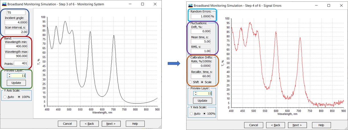
Fig. 4.Left panel: Step 3 of the BBM Simulator; Right panel: Step 4 of the BBM Simulator. Errors in measurement data. Spectral characteristics are displayed for layer number 11. |
|
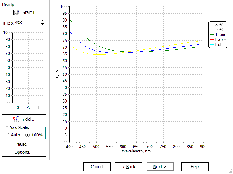
Fig. 5. Computational deposition run. At the fifth step of the dialog, the deposition runs controlled by the BBM are performed. In the course of computational manufacturing experiments, successive on-line measurement data scans are analyzed by the incorporated control algorithm in order to determine termination times for layer depositions. |
The running heading above the Start button indicates what layer is currently deposited. Three bars below the Start button indicate theoretical layer thickness (green), growing thickness of the deposited layer (aqua), and estimated thickness of the deposited layer (red). The last thickness is estimated by the on-line characterization algorithm on the basis of on-line monitoring data shown by the red spectral curve in the right part of the window. The estimated thickness value is used by the control algorithm to make a decision about terminating layer deposition. The green spectral curve (right panel) represents a theoretical spectral transmittance/reflectance at the end of the current layer deposition. This curve corresponds to the thickness of the current layer indicated by the green bar at the left panel. The yellow spectral curve is a theoretical curve when 80% of the current layer thickness is deposited and the blue curve is a theoretical curve when 90% of the current layer thickness is deposited. The aqua spectral curve is transmittance/reflectance corresponding to the actual thickness of the current layer. This thickness is represented by the aqua bar at the left part of the window. The Pause checkbox regulates whether there are time intervals between depositions of layers or not. The Y Axis Scale radio button allows selecting the type of scaling for the preview screen. |
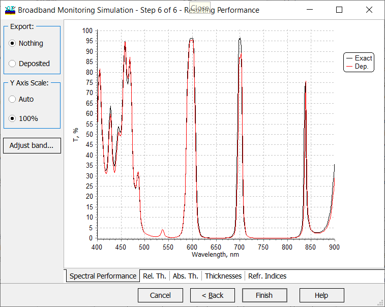
Fig. 6. Result of a deposition run of a 31-layer two-line filter with settings from Figs. 3-4. Transmittance degrades definitely around the wavelength 700 nm. |
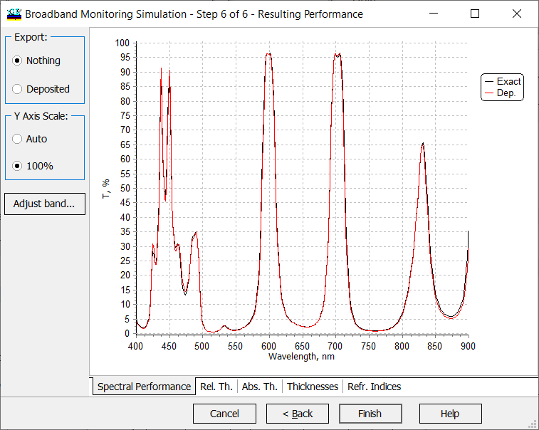
Fig. 7. Result of a deposition run of a 27-layer robust two-line filter with settings from Figs. 3-4. |
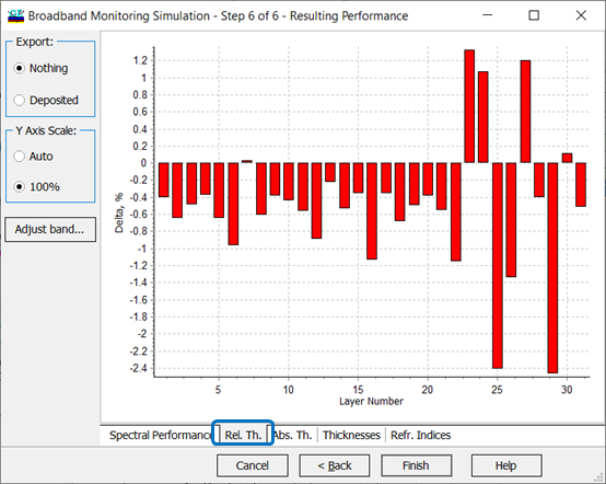
Fig. 8. At the sixth step, actual errors in layer thicknesses are displayed. |
Rel.Th. tab (Fig. 8) allows to represent obtained relative thickness errors in the form of bar chart. Abs.Th. tab is quite similar, but represents obtained thickness errors as absolute values. The Thicknesses tab allows previewing relative errors in layer thicknesses of the simulated coating. The Thicknesses tab allows the user to examine results of the computational manufacturing experiment in numerical form. There you can find physical thicknesses of layers of theoretical design, actual physical thicknesses of layers, relative and absolute errors in layer thicknesses of the simulated coating. Refr. Indices tab displays information concerning variations of refractive indices and inhomogeneities during simulated deposition. The Export field at the left panel can be used for exporting actually deposited design to the memory. This design is exported after pressing the Finish button if the Deposited radio button is checked. The exported design can be then processed using other OptiLayer options. |
| BBM option allows you to perform a number of simulated runs a number of times and to estimate the production yield that is defined as the ratio of successful deposition runs to the total number of runs. The production yield is a number from 0 to 100%.
A deposition run is successful if its spectral characteristics lie in the allowed corridor that is defined through the range target. If you have a series of design solutions of the same problem, it is recommended to perform 10-20 computational runs for each solution. If a solution exhibits a low yield or a medium, it is recommended to exclude this solution from the consideration. For solutions exhibiting almost 100% yield, further tests should be performed, for example, 100-200 runs. |
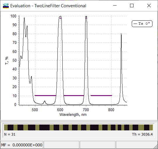
Fig. 9. A 31-layer two-line filter and the range target. |
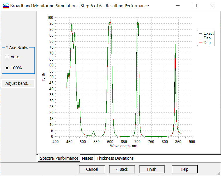
Fig.10. Resulting performances of 10 simulation runs of the 31-layer two-line filter. |
Successful design spectral characteristics are plotted in green color, spectral characteristics of designs that are at least partly outside of the corridor specified with range target are plotted in red color (Fig. 10). It is possible to terminate computations at any moment. Computational progress is represented by the progress indicator in the status bar of the Broadband Monitoring Yield (Fig.11). Relative part of successful design is represented as percentage at the second progress indicator.
|
| Of course, you can enlarge the critical spectral ranges (Fig. 11).
On the misses tab, Upper misses (events when the spectral curve violated upper boundary of specifications) are represented as a blue area, lower misses (events when the spectral curve violated lower boundary of target values) are represented as a green area. Total number of misses for each wavelength is represented by the red curve. |
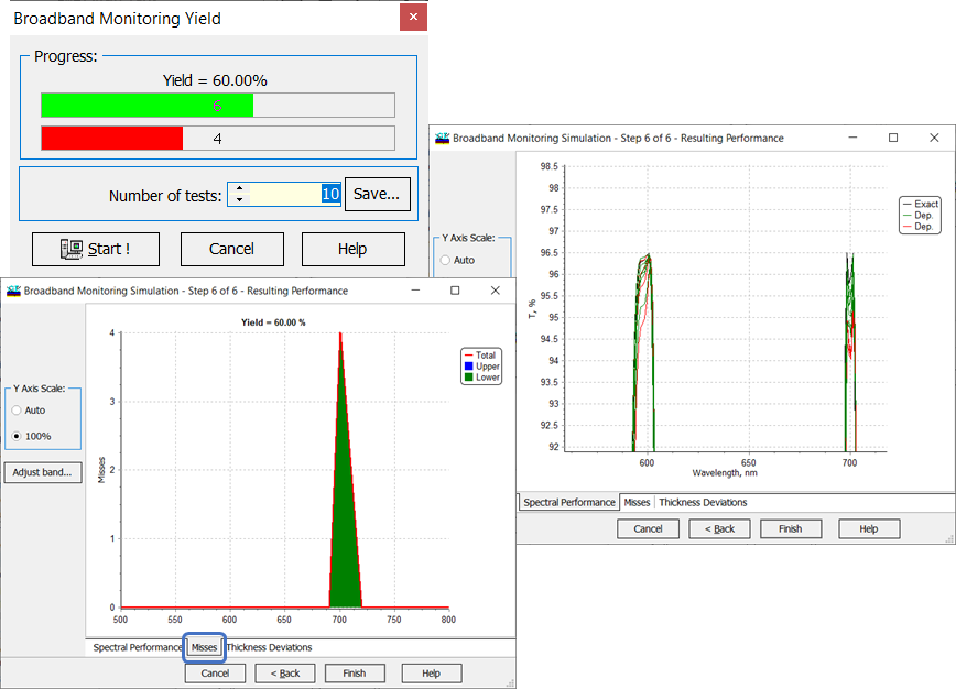
Fig. 11. Summary of the yield analysis: 60% deposition runs are successful, the most critical spectral range is around the wavelength 700 nm. |
You may be interested in the following articles:
|
|
|
References
|
|
OptiLayer provides user-friendly interface and a variety of examples allowing even a beginner to effectively start to design and characterize optical coatings. Read more…
Comprehensive manual in PDF format and e-mail support help you at each step of your work with OptiLayer.
If you are already an experienced user, OptiLayer gives your almost unlimited opportunities in solving all problems arising in design-production chain. Visit our publications page.
Look our video examples at YouTube
OptiLayer videos are available here:
Overview of Design/Analysis options of OptiLayer and overview of Characterization/Reverse Engineering options.
The videos were presented at the joint Agilent/OptiLayer webinar.