
|
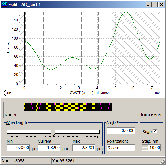
Evaluation of the standing wave electric fields inside a stack of films is effected with the Field command from the Analysis Menu. This distribution may be useful in the course of solving complicated design problems. OptiLayer computes the electrical field intensity inside the current design and plots it in the graphical form. The physical thickness profile of the layers in the design is represented by the design bar displayed just below the graph of electric field strength. The design bar shows the different layer materials in different colors and/or patterns, the number of layers N and the overall thickness Th of the coating design. You can select the wavelength value at which you want to see the electric field distribution by moving the slider in the Wavelength frame. The overall spectral range for the slider is shown (and can be modified) in the Min and Max fields; the current position of the slider is displayed as the wavelength value in the Current field. You can limit the slider to a specific set of wavelength values if you check the Snap box at the right of the window. When the Snap box is checked, the slider can stop only at positions defined by the minimum and maximum wavelength values and the increment defined in the Step edit field. Note that the increment is always set in nanometers, and must be in the range from 1 to 100. You can also set the Angle of incidence and Polarization state (S, P or Both) in the corresponding edit boxes. \(|E|^2\) values are expressed in relative units when incident wave has \(|E|^2=100\%\). Since these values are quadratic, \(|E|^2\) can reach 400% in the incident medium for the case of high reflectors. |
 |
 |
 |
OptiLayer provides user-friendly interface and a variety of examples allowing even a beginner to effectively start to design and characterize optical coatings. Read more…
Comprehensive manual in PDF format and e-mail support help you at each step of your work with OptiLayer.
If you are already an experienced user, OptiLayer gives your almost unlimited opportunities in solving all problems arising in design-production chain. Visit our publications page.
Look our video examples at YouTube
OptiLayer videos are available here:
Overview of Design/Analysis options of OptiLayer and overview of Characterization/Reverse Engineering options.
The videos were presented at the joint Agilent/OptiLayer webinar.